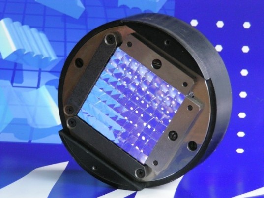
Basic specifications

Material: Fused Silica, Optical Glass, Plastics
Spectral range: 193 nm to 3.5 μm
Micro Lens Dimension: 10 μm to 4000 μm
Functional Lens Shape: Positive, Negative; Spherical, Aspherical
Surface Roughness: less than 10 Angstrom ( Å )
Numerical Aperture: 0.004 - 0.45
Lens Positioning: down to ± 0.2 μm
Focal Lenght Variation: ± 2% within 100 mm array dimension
Array Dimension: Typically 4'' x 4'', up to 6'' x 6''
Packing Density: above 90 %
Array Pattern: Hexagonal, Orthogonal, Square, Circular,
Cylindrical, Irregular, etc.
Key advantages of [aμs] Microoptics vs. Standard Optics
Highly Effective Shaping of Beam Cross Section.
- Shapes beam into line-, cross- or other beam cross sections.
Highly Efficient Intensity Profiling.
- Generates specified intensity profile over cross section, e.g. Gaussian or flat top.
Simple and Highly Efficient Beam Multiplexing.
- Adds speed and accuracy to multichannel processing.
Highly Effective Bundling of Multiple Beams.
- One general beam is gathered from several sources, for projection TV, light shows etc.
Efficient Collimation of Diode Laser Emission.
- Fast axis collimation with high NA lenses, slow axis collimation and bundling.
Higher Efficiency of Photosensitive Devices.
- Beam is focused directly onto the focus-sensitive pads of CCD-matrices.
Higher Effectiveness of Fiber Systems.
- Beam is focused into fiber core for opto-sensorics, fiber coupling, optical switching, etc.
Higher Precision of Measuring Systems.
- Uses exactly positioned monolytic test structures, such as focusing or alighment sensors, distance, depth and size measuring devices.
Improvement of Traditional Optical Schemes.
- Relates to size, weight, cost, sensitivity, stability and precision, especially in microphotolithography, consumer products, office equipment, etc.
Novel Optical Schemes.
- Supports 3D photography, confocal microscopy, optical computing and integral microtechniques.

